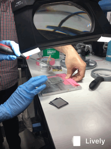
Our REU student Canisha is working on large-scale and small-scale versions of a design for an electrical contact system. “Large-scale” means assembling millimeter-scale components to a circuit board using solder paste, which she is stenciling above. In printed circuit board assembly, stenciling is followed by robotic placement of small components like resistors and diodes. “Small-scale” on this project means drawing micron-to-mm scale patterns on a photomask. One of the designs we are working on is below, but there are many more creative variants on this mask! A photomask is the starting point for photolithography, a process that prints the components side-by-side on a silicon wafer instead of assembling them individually. While we are using our photomask to make micromechanical structures, the same machines we use to pattern metal and insulating layers are used in the semiconductor industry to make chips.
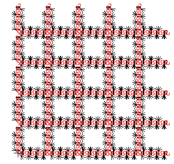
Photomask pattern: each square in the grid is approximately 1.5mm x 1.5mm