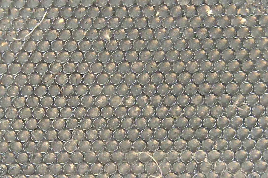
The fall Materials Research Society meeting was a hybrid of in-person and remote presentations. Here is our work on characterizing a soft, micromolded silicone layer for its pressure-dependent optical properties. Independent Study students Michael Portaro and Rio Brittany, both in ECE, developed different parts of the project during 2021. The end result was a material that lets increasing amounts of light through when pressure is increased from 0 to 2 PSI. Applications of this microstructured material include touch sensors for soft robotic hands and human-computer interfaces.
Student has a solid grasp of the material

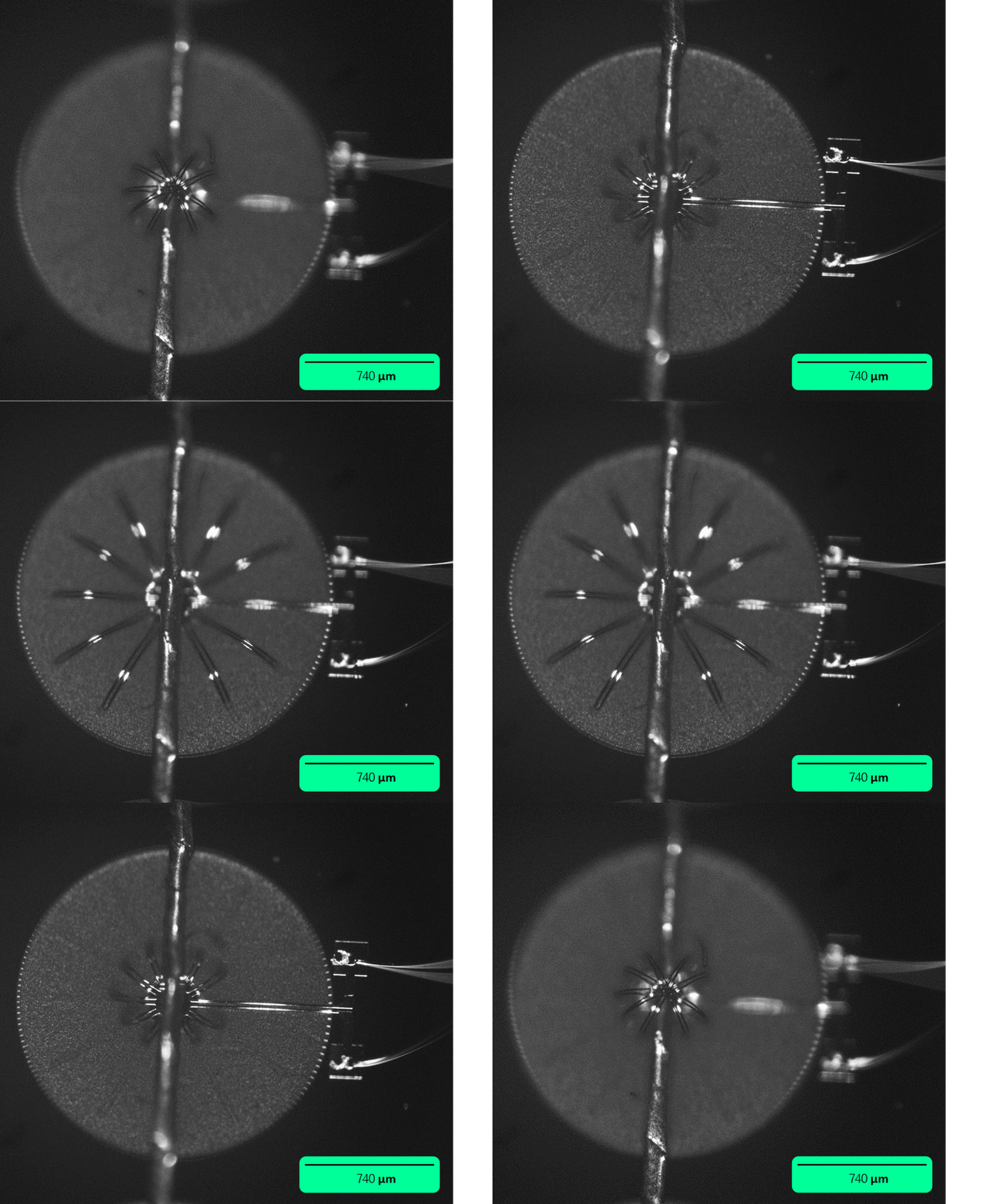
Research Experience for Undergraduates (REU) Student Muhemmad Yassin got a microelectromechanical (MEMS) gripper to grasp this conductive fiber as part of his summer research in the IMPACT REU program. This project aims to create a porous, breathable packaging system for MEMS in wearable and flow-through applications. Muhemmad is now taking the project on the road at the IMPACT convocation where dozens of students from different cleanroom REU sites meet. If you’re interested in participating next year, get in touch using the “Join the Lab” link.
A gripping presentation
Here is Sushmita’s talk from the 2021 Manufacturing Science and Engineering Conference on designing microelectromechanical system (MEMS) layouts that align with one-of-a-kind structures like a piece of fabric. Most fabrics do have a uniform and predictable structure that can be described by a measurement such as “threads per inch.” However, threads do not have the submicron dimensional accuracy of a MEMS layout on a silicon wafer. Threads are soft, often made from natural fibers that vary from batch to batch, and conditions such as tension during assembly control the tightness of the weave or knit. Therefore, on the microscale, each piece of fabric is different. In this presentation, images of individual fabric pieces are processed to generate a MEMS gripper layout that will attach microdevices to specific fibers in the swatch. The focus of this research is on automated image processing methods that quickly identify good gripper locations. The desired result is a technology that lets engineers use flexible, porous, multimaterial fabrics as new packaging materials for MEMS devices.
Breaking the Mold
Interested in soft robotics made from a diverse array of materials? Attend the SCRAMbots virtual workshop on April 12 at the 2021 RoboSoft conference! Registration is free. Speaker information, registration, and poster session details here: https://www.scrambots.com/robosoft-workshop-2021
Careful with those nanoplates

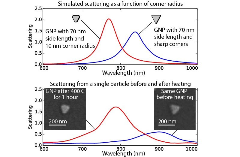
Our collaborative work on thermal processing of gold nanoplates with the O’Toole group (U of L Bioengineering) is accepted (update: published) at Materials Letters. We’ve used their triangular gold nanoplates to induce local heating of microelectromechanical (MEMS) structures with infrared lasers. The nanoplates are typically the first layer to go onto the MEMS wafer. In this paper, we show that temperatures in the 200-300 C range can shift the absorbance wavelength of the nanoplates by rounding the corners, far lower than the melting temperature of bulk gold (>1000 C). Thanks to careful mapping, Jaz and Kurtis were able to find the same tiny nanoplates (70 nm side lengths) before and after heating, in both electron and optical microscopes. Temperatures reach the 200-300 C range during MEMS processing unless you take care to use low-temperature materials and methods. So, when using gold nanoplates, either keep your cool or prepare for them to behave differently in the final device — absorbing shorter wavelengths than they started with.
